-
-
-
PCB Production Main Materials
PCB Machine Spares
FPC Production Materials
-
-
PCB PISM Ink Photoimageable Solder Mask Ink
201 this series of inks are two-component screen printing liquid photosensitive solder masks ink, suitable for high-precision printed circuit boards, with high resolution, excellent heat resistance and chemical resistance.
PCB Production Main Materials
PCB PISM Ink Photoimageable Solder Mask Ink

![]()
Liquid Photoimageable Solder Mask Ink 201 Series
201 this series of inks are two-component screen printing liquid photosensitive solder masks ink, suitable for high-precision printed circuit boards, with high resolution, excellent heat resistance and chemical resistance.
1. Product Model
| Item Name | Color | |
|
PISM INK |
201GA | Light Green (Yellowish phase) |
| 201GB | Medium Green(Yellowish phase) | |
| 201GC | Matte Green (Bluish phase) | |
| 201W | White | |
| 201BK | Black | |
| 201R | Red | |
| 201Y | Yellow | |
| 2.201BU | Blue | |
| 201V | Purpose | |
2. Physical Characteristic
| Item | Characteristic | Remarks |
| Fineness | ≤8μm | 0~25μm (Scraper fineness meter) |
| Mixing ratio | Main agent/hardener = 750:250 | Weight ratio |
| Main Ink Viscosity | 210±40dPa’s | VT-04E viscometer (25℃) |
| Nonvolatile component | 70-72wt% | After Mixing |
| Precuring Range | 75℃/55mins | Max. |
| Properly Expose Energy | 300~600mj/cm² | Energy on the Ink surface |
| Storage Time after Mixing | 24 hours | ≤25℃ dark Place |
| Storage Life | 6 months | ≤25℃ dark Place |
| Exposure energy | 600-900mJ /cm² | UV energy |
| Packaging | main agent: 750g; curing agent: 250g |
conventional packaging |
Thinner additive amount is about 0~30ml/kg (Please using our special thinner)
3. Pre-curing Range
| 75℃ | 30mins | 40mins | 50mins | 60mins |
|
Development |
0 | 0 | 0 | 0 |
Development Condition: 1%Na2CO4 30℃, 40~60secs, 1.8~2.0Kg/cm², “0” means OK
4. Shelf Test (75℃, 25 mins after pre curing)
| Time | 12 hr | 24 hr | 36 hr | 48 hr |
|
Development |
0 | 0 | 0 | 0 |
Environment: 22℃, 66%RH, “0” means OK
5. Photosensitive Property
| Item | Ink Thickness | Exposing Power | Development Time | Exposing Grade |
|
21 Grade Exposing Scale |
25μm |
300mj/cm²~600mj/cm² |
40~60 secs |
9~11 Grades |
6. Operating Procedures
| Procedure | Condition |
| CCL Surface Treatment | Standard Acid Processing and Brushing |
| Ink Mixing | Mixing the Main ink and the harder, manual/auto mixing and let it stand for 10 mins |
| First side printing | 36~51T screen mesh, after printing let it stand for 10 mins |
| Pre-baking | 70~75℃ 15~20 mins |
| Second Side Baking | 70~75℃ 25~35 mins |
| Exposing | 300~600mj/cm², 9~11 grade (21 grade scale) |
| Standing Time | 10 mins |
| Developing | 1% Na₂CO₃30℃ 45~55secs, Pressure 1.5~2Kg/cm² |
| Post-baking | 150℃, 60mins |
If using Double Side Printing, the pre-baking time should be 25~35 mins.
7. Chemical Resistance
| Chemical | Dipping Time | Result |
| Isopropanol | Room Temp. 20mins | Normal |
| Methylbenzene | Room Temp. 30mins | Normal |
| Sulfuric Acid (10%) | Room Temp. 30mins | Normal |
| Hydrochloric Acid (10%) | Room Temp. 30mins | Normal |
| Sodium Hydroxide(10%) | Room Temp. 30mins | Normal |
| 1.1.1.Trichloroethane | Room Temp. 30mins | Normal |
| Environmental Standards | Comply with ROHS directive | SGS Pass |
8. Physical Property
| Items | Performance | Testing Condition |
| Coating Hardness | >6H | IPC-SM-840B 3.5.1.2. (MITSUBISHI PENCIL) |
| Wear-resisting property | Normal | IPC-SM-840B 3.5.1.1. |
| Surface adhesion | Normal | IPC-SM-840B 3.5.2. to Gold or Nickel and tin |
| Machinability | Normal | IPC-SM-840B 3.5.3.Drilling/Punching Testing |
| Heat Resistance | 260℃±5℃ 10secs*3 times | JIS C6481 5.5 |
| Combustibility | UL94 V-0 | IPC-SM-840B 3.6.4. |
9. Electrical Specification
| Items | Performance | Testing Condition |
| Insulation breakdown voltage | 1000V De/mil | IPC-SM-840B 3.8.1. |
| Volume Resistance | 1 x 10¹⁵Ω | ASTM D-257 ASTM D-257 |
| Surface Resistance | 1 x 10¹⁵Ω | IPC-SM-840A 3.8.2. |
| Insulation Resistance | 1 x 10¹⁵Ω 1 x 10¹⁵Ω 1 x 10¹⁵Ω |
Class 1 35℃ 90% RH 4 Class 2 50℃ 90% RH 7 Class 3 25~65℃ 90% RH 7 |
| Dielectric dissipation factor | 0.02 | JIS C6481 1MHz |
10. Note
1) Operating environment requirements: printing room and exposure room, the temperature must be 22 ℃ ± 2 ℃, temperature 55-65% in a dust-free room, in addition, if used directly or indirectly under white light or sunlight, it will cause ink Photopolymerization reaction, so please work without UV light.
2) When the ink temperature returns to room temperature, then can be opened and used, mixed with the specified amount of hardener(Curing Agent), fully stirred and stand for use.
3) The thickness of the ink is preferably 20-25um. If the film thickness is thin, it is easy to reduce the solder heat resistance, chemical resistance and the need for gold plating ability. If the coating film is too thick, the exposure not enough to complete the exposing, which is easy to occur Excessive side erosion and reduced dryness.
4) Printing can not directly paste the adhesive cloth, it is easy to have residual glue and cause dents on the board surface.
5) When printing, pay attention to avoid printing ink into the hole. If the ink is printed into the hole, the development time must be prolonged, otherwise, it will make the hole inside development unclean.
6) The pre-bake conditions and the allowable range of pre-bake will vary with the type of oven and the number-quantity of PCB in the oven. Therefore, it is necessary to perform confirmation experiments before setting appropriate conditions.
7) The exposure energy will vary depending on the PCB material and the thickness of the coating film, so experiments are required to confirm the minimum residual width of the ink, surface gloss and backside sensitivity, and then set appropriate conditions.
8) Water green/ White/ black color, the exposure energy should be increased, otherwise it will easily cause cracks after development and after baking, and will be broken.
9) When the developing temperature and time are insufficient, the developing will be unclean, and the phenomenon of excessive side erosion will easily occur when the developing temperature and time are exceeded, and the surface of the ink will be attacked and affect the ink features. Please strictly control the concentration of the developing wave/ temperature/ nozzy pressure/time, so it is necessary to perform confirmation experiments before setting appropriate conditions.
10) When the post-baking temperature is insufficient in time, the tin spraying will cause paint peeling, and excessively will reduce the gold plating resistance. Therefore, after confirming the experiment, set the appropriate conditions for tin spraying and gold plating.
11) After the hole plugging, it must be baked in sections: 80℃×30min, 100℃×30min, 150℃×50min.
12) If you need to print legend ink, please pay attention to setting the baking time after solder mask suitable for legend ink, otherwise insufficient hardening will reduce the characteristics of the ink coating.
13) When the PCB is electrolessly gold-plated, it is best to first gold plating and then print the legend ink, otherwise the gold-plating resistance will be reduced when the hardening is excessive.
![]()
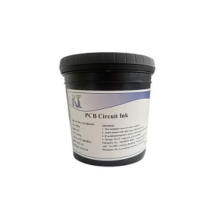
PCB Circuti Ink(Etching Resist Ink), Marking Ink, Peelable Solder Mask Ink etc......
![]()


* Original Manufacturing Supply

* Professional Team

* Better Quality

* Better Pre-sales & After-sales Service

* Fast Delivery

* Technology Support

Shenzhen Kewei Industries Limited has nearly ten years of production and sales experience in PCB auxiliary materials, and has formed eight series of more than 200 varieties, including Artwork Film, PCB Tools, Drill Backup board/ Entry Sheet, PCB Ink, Wet Process Chemical, Dry Film, Machine Spares and Other production consumables. We have full and complete production materials for Rigid PCB Factory/ Multi-layer Factory/ FPCB factory. Also we provide Machine Spindle Services, PCB factory setup / upgrade solution by our experienced team. We aim to provide "one-stop" services to all the PCB factory.
![]()
Shenzhen Kewei Industries Limited
Kewei Industries (HK) Limited
Email: sales5@sz-kewei.com; support@sz-kewei.com
Tel/Fax: 0086-769-22211186
Mob: 0086-13537348123
All copyright © Shenzhen Kewei Industries Limited


